Alloy 42,Low expansion 42 Alloy Strip,UNS K94100,E FORU
Product Code : NI-S840-CU-CU
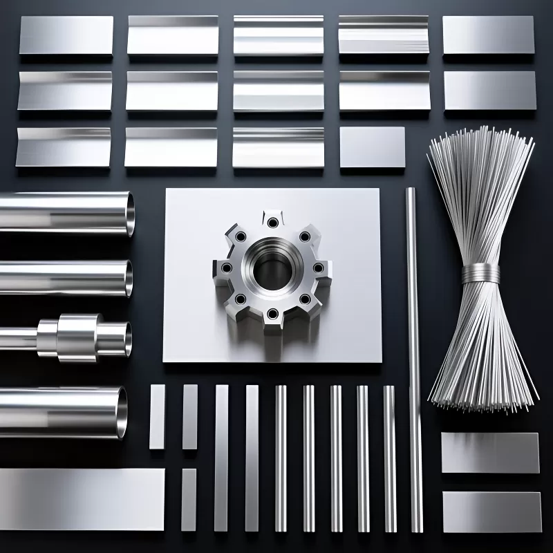
Alloy 42,Low expansion 42 Alloy Strip,UNS K94100, is available in Bar (Round bar, Flat bar), Ribbon, Wire, Rods, Tube, Pipe, Foil, Plate, Sheet, Strip and Forging Stock.
Please contact us if you need customized services. We will contact you with the price and availability in 24 hours.
British Specs:,American Specs: ASTM F30
ASTM B 753
AMS 5683 Welding Wire,German Specs: WS 1.3917,DIN 17745
AFNOR NF A54-301
**PRODUCT DATASHEET: ALLOY 42 / LOW EXPANSION 42 ALLOY STRIP**
**UNS K94100 - Precision Strip Product**
---
### **1. OVERVIEW**
**Alloy 42**, commercially known as **Low Expansion 42 Alloy**, is a precision **nickel-iron alloy** containing **42% nickel** that delivers an exceptionally **low coefficient of thermal expansion (CTE)**, specifically engineered to match **borosilicate glass, alumina ceramics, and critical semiconductor materials**. Supplied in **precision strip** form, this product offers exceptional dimensional stability and formability for high-volume manufacturing of precision electronic components. The alloy is registered under the Unified Numbering System as **UNS K94100**.
---
### **2. CHEMICAL COMPOSITION (Weight %)**
| Element | Alloy 42 Strip Specification | UNS K94100 Requirements |
|------------------|------------------------------|-------------------------|
| **Nickel (Ni)** | 41.0 – 42.5% | 41.0 – 42.5% |
| **Iron (Fe)** | Balance | Balance |
| **Manganese (Mn)**| 0.50 – 0.80% | ≤ 0.80% |
| **Silicon (Si)** | 0.15 – 0.30% | ≤ 0.30% |
| **Carbon (C)** | ≤ 0.05% | ≤ 0.05% |
| **Chromium (Cr)**| ≤ 0.15% | ≤ 0.15% |
| **Copper (Cu)** | ≤ 0.05% | ≤ 0.05% |
| **Aluminum (Al)**| ≤ 0.05% | ≤ 0.05% |
| **Sulfur (S)** | ≤ 0.015% | ≤ 0.015% |
| **Phosphorus (P)**| ≤ 0.015% | ≤ 0.015% |
---
### **3. PHYSICAL & MECHANICAL PROPERTIES**
| Property | Annealed Condition | Half-Hard Condition |
|---------------------------------|--------------------|---------------------|
| **CTE (20–300°C)** | 4.5 – 5.5 × 10⁻⁶/°C | 4.5 – 5.5 × 10⁻⁶/°C |
| **Density** | 8.11 g/cm³ | 8.11 g/cm³ |
| **Tensile Strength** | 450 – 550 MPa | 550 – 650 MPa |
| **Yield Strength (0.2% Offset)**| 250 – 350 MPa | 450 – 550 MPa |
| **Elongation (in 2")** | 35 – 45% | 8 – 15% |
| **Hardness (Rockwell B)** | 65 – 75 HRB | 85 – 95 HRB |
| **Electrical Resistivity** | 0.75 μΩ·m | 0.75 μΩ·m |
| **Thermal Conductivity** | 14.5 W/m·K | 14.5 W/m·K |
| **Modulus of Elasticity** | 145 GPa | 145 GPa |
---
### **4. INTERNATIONAL STANDARDS & EQUIVALENTS**
| Standard Organization | Designation & Specification |
|-----------------------|----------------------------|
| **UNS** | K94100 |
| **ASTM** | F30 (Alloy 42) |
| **EN (European)** | 1.3917 (Ni42Fe) |
| **ISO** | NiFe42 |
| **JIS (Japan)** | C42N |
| **GB (China)** | 4J42 |
| **DIN (Germany)** | Ni42 |
| **Strip Standards** | ASTM B749, AMS 7721 |
---
### **5. STRIP SPECIFICATIONS**
#### **5.1 Dimensional Range**
- **Thickness**: 0.05 mm to 2.0 mm (±0.002 mm to ±0.02 mm)
- **Width**: 2.0 mm to 600 mm (±0.02 mm to ±0.2 mm)
- **Length**: Coils up to 5000 meters, cut lengths available
- **Camber**: ≤ 1 mm per 2 meters
#### **5.2 Temper Conditions**
- **Annealed (Soft)**: Optimal for severe forming and deep drawing
- **Quarter-Hard**: Good formability with moderate strength
- **Half-Hard**: Balanced formability and spring properties
- **Hard**: Maximum strength for spring applications
#### **5.3 Surface Finish**
- **Standard Matte**: Ra 0.4-0.8 μm
- **Bright Annealed**: Ra 0.1-0.3 μm
- **Skin-Passed**: Improved flatness and surface texture
- **Special Finish**: Custom surface treatments available
---
### **6. PRODUCT APPLICATIONS**
#### **6.1 Electronics & Semiconductor**
- **Lead Frames**: IC, transistor, and diode lead frames
- **Connector Components**: Electronic connector contacts
- **Semiconductor Packaging**: Chip carrier substrates
- **Hybrid Circuit Bases**: Thin-film circuit substrates
#### **6.2 Automotive Electronics**
- **Sensor Elements**: Automotive sensor components
- **ECU Components**: Electronic control unit parts
- **Ignition Parts**: Ignition system components
- **Power Electronics**: Power module substrates
#### **6.3 Consumer Electronics**
- **Battery Contacts**: Spring contact components
- **Display Components**: Flat panel display parts
- **Communication Devices**: Mobile device components
- **Audio Equipment**: Speaker and audio components
#### **6.4 Telecommunications**
- **RF Components**: Shielding and contact elements
- **Fiber Optics**: Alignment and structural components
- **Connector Systems**: Precision connector parts
- **Switching Devices**: Relay and switch components
---
### **7. PROCESSING CHARACTERISTICS**
#### **7.1 Stamping & Blanking**
- **Fine Blanking**: Excellent for precision components
- **Tool Clearance**: 5-8% of material thickness
- **Burr Height**: Controlled to ≤ 0.02 mm
- **Production Rates**: Suitable for high-speed stamping
#### **7.2 Forming & Deep Drawing**
- **Deep Drawing**: Excellent in annealed condition
- **Bend Radius**: Minimum 0.5× thickness
- **Springback**: Predictable and consistent
- **Work Hardening**: Moderate rate
#### **7.3 Etching & Chemical Processing**
- **Photoetching**: Ideal for precision etched components
- **Etch Factor**: Typically 1:1 to 1:1.5
- **Etchants**: Compatible with standard etching chemicals
- **Tolerance**: ±0.01 mm for etched features
---
### **8. QUALITY ASSURANCE**
#### **8.1 Dimensional Control**
- **Thickness Monitoring**: Laser gauge continuous monitoring
- **Width Control**: Precision slitting with edge monitoring
- **Flatness**: Controlled to ≤ 3 mm/m
- **Surface Quality**: 100% visual inspection for critical grades
#### **8.2 Material Testing**
- **Chemical Analysis**: Certified for each melt heat
- **Mechanical Testing**: Regular tensile and hardness verification
- **Surface Roughness**: Controlled per specification requirements
- **Grain Size**: ASTM 7-9 for optimal formability
#### **8.3 Certification**
- **Material Certificates**: EN 10204 3.1/3.2
- **Traceability**: Complete lot traceability maintained
- **Process Control**: Statistical process control implemented
- **Custom Testing**: Application-specific testing available
---
### **9. TECHNICAL ADVANTAGES**
- **Perfect CTE Match**: Excellent thermal compatibility with glass and ceramics
- **Superior Formability**: Ideal for high-speed stamping and forming
- **Excellent Surface Quality**: Suitable for precision electronic applications
- **Consistent Properties**: Reliable performance in volume production
- **Good Weldability**: Compatible with resistance and laser welding
- **Thermal Stability**: Maintains dimensions across temperature ranges
---
### **10. PACKAGING & DELIVERY**
#### **10.1 Standard Packaging**
- **Coil Packaging**: Wooden or steel reels with edge protection
- **Width Protection**: Custom spacers for precision widths
- **Surface Protection**: VCI paper and plastic wrapping
- **Identification**: Continuous marking with specifications
#### **10.2 Special Requirements**
- **Cleanroom Packaging**: Class 1000 environment available
- **ESD Protection**: Anti-static packaging materials
- **Dry Atmosphere**: Nitrogen purging for sensitive applications
- **Just-in-Time**: Scheduled delivery programs
---
**Note:** For high-volume precision stamping applications, technical consultation is recommended to optimize material selection and processing parameters. Sample material and technical support available for process development and tooling design. Custom tempers and special testing available upon request.
Packing of
Standard Packing:
Typical bulk packaging includes palletized plastic 5 gallon/25 kg. pails, fiber and steel drums to 1 ton super sacks in full container (FCL) or truck load (T/L) quantities. Research and sample quantities and hygroscopic, oxidizing or other air sensitive materials may be packaged under argon or vacuum. Solutions are packaged in polypropylene, plastic or glass jars up to palletized 2463 gallon liquid totes Special package is available on request.


,INCONEL alloy 725,1")